AED 8.30
Description
The 74LS112 IC is a versatile dual JK flip-flop. It features two distinct negative-edge-triggered J-K flip-flops, each equipped with individual J-K inputs, clock inputs, and inputs. This IC operates effectively over a wide range of voltage and conditions and offers seamless interfacing capabilities with CMOS, NMOS, and TTL technologies. The output of the 74LS112 IC is consistently in TTL format, simplifying its compatibility with other TTL devices and microcontrollers.
Package Includes:
- 1x dual JK flip-flop 74LS112 IC
Features:
- Dual JK Flip-Flop: The 74LS112 IC is equipped with two independent JK flip-flops, allowing for versatile logic operations.
- Negative-Edge-Triggered: These flip-flops are negative-edge-triggered, ensuring precise timing and synchronization with external signals.
- Individual Inputs: Each flip-flop includes individual J-K, clock, and direct clear inputs, enhancing control and flexibility in circuit design.
- Wide Voltage Range: The IC operates over a wide range of working voltages, making it adaptable to various voltage conditions.
- Universal Compatibility: It directly interfaces with CMOS, NMOS, and TTL technologies, facilitating seamless integration into different electronic systems.
- Consistent TTL Output: The IC consistently outputs in TTL format, simplifying compatibility with other TTL devices and microcontrollers.
- Clock Circuitry: The JK Flip-Flop within the IC incorporates clock input circuitry, enabling synchronized operations and preventing invalid conditions.
- Multiple Input Combinations: With clocked input, it offers four input combinations: "logic 1", "logic 0", "No change", and "Toggle," allowing for a range of logical operations.
Description:
The 74LS112 IC is a dual JK flip-flop known for their versatility in digital logic circuits. These flip-flops are negative-edge-triggered, ensuring precise timing and synchronization with external signals. Each flip-flop boasts individual J-K inputs, clock inputs, and direct clear inputs, enhancing control and flexibility in circuit design. One of its remarkable attributes is its ability to operate efficiently over a wide range of working voltages and conditions. This adaptability makes it a suitable choice for various electronic applications. Furthermore, the 74LS112 IC offers seamless interfacing capabilities with CMOS, NMOS, and TTL technologies, allowing for easy integration into diverse electronic systems. One key advantage is the consistent TTL output, simplifying compatibility with other TTL devices and microcontrollers. Inside the IC, clock input circuitry is integrated, enabling synchronized operations and preventing invalid conditions. It also provides four input combinations: "logic 1," "logic 0," "No change," and "Toggle," which expand its utility for a wide range of logical operations, making it an essential component in digital electronics.
Principle of Work:
the 74LS112 IC operates using JK flip-flops, and understanding how it works internally can help you comprehend its functionality within a circuit.
Internal Operation:
- JK Flip-Flops: The IC contains two JK flip-flops. Each flip-flop has two inputs: J (set) and K (reset), a clock input (CLK), and a direct clear input (CLR). These flip-flops can store binary information in the form of a 0 or 1.
- Clock Triggering: The flip-flops are negative-edge-triggered, which means they respond to the falling edge of the clock signal. When the clock signal transitions from high to low (1 to 0), the flip-flops sample the values of J and K inputs and update their states accordingly.
- Logic Operations: The J and K inputs control the behavior of the flip-flops. The specific logic states on these inputs determine whether the flip-flops will toggle, set, reset, or remain in their current state. The combination of J and K inputs creates a truth table that defines the behavior of the flip-flops.
- Clear Input: The CLR input allows you to clear or reset the flip-flop to a known state when asserted.

Operation within a Circuit: When you use the 74LS112 IC within a circuit, you typically connect it to other components to perform specific logical functions or store binary information:
- Input Signals: You provide appropriate logic signals to the J and K inputs of each flip-flop. These signals determine the desired logical operation (set, reset, toggle, or hold) for each flip-flop.
- Clock Signal: The clock input (CLK) receives a clock signal. When the clock signal transitions from high to low (falling edge), the flip-flops respond to the logic signals at the J and K inputs and update their states accordingly.
- Output Signals: The Q and Q' outputs of the flip-flops reflect their current states. These outputs can be connected to other components in the circuit to perform specific tasks, such as controlling other logic gates, storing binary data, or generating sequential logic sequences.
- Clear Functionality: The clear input (CLR) allows you to reset the flip-flops to a predefined state when needed. This can be useful for initializing the circuit or resetting it to a known condition.
Pinout of the IC:
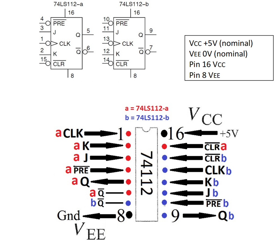
| Pin Name | Pin No. | Description |
|---|---|---|
| 1CLK | 1 | Clock Input 1 |
| 1K | 2 | Input Pin K1 |
| 1J | 3 | Input Pin J1 |
| 1PRE’ | 4 | Active low Preset Pin 1 |
| 1Q | 5 | Output pin Q1 |
| 1Q’ | 6 | Active Low output Pin Q1 |
| 2Q’ | 7 | Active Low output Pin Q2 |
| GND | 8 | Ground Pin |
| 2Q | 9 | Output pin Q2 |
| 2PRE’ | 10 | Active low Preset Pin 2 |
| 2J | 11 | Input Pin J2 |
| 2K | 12 | Input Pin K2 |
| 2CLK | 13 | Clock Input 2 |
| 2CLR’ | 14 | Active low clear/Reset pin 2 |
| 1CLR’ | 15 | Active low clear/Reset pin 1 |
| Vcc | 16 | Chip Supply Voltage |
Applications:
- Frequency Division: It can be used to divide the frequency of a clock signal by toggling its output state based on specific input conditions. This is useful in creating frequency dividers and counters.
- Sequential Logic: The IC is essential for building sequential logic circuits like shift registers, binary counters, and state machines. It helps control the sequence of events in digital systems.
- Memory Elements: It can serve as a basic memory element in microcontrollers and microprocessors for storing temporary data or controlling program execution.
- Data Synchronization: In communication systems, it's employed to synchronize data transmission and reception, ensuring that data is sampled at the correct time.
- Control Signals: It's used to generate control signals in various applications, such as controlling the read and write operations in memory devices or as part of control logic in microcontrollers.
- Logic Functions: The IC can be configured to implement various logic functions, including AND, OR, NOT, and XOR, by appropriately setting the J and K inputs.
- Frequency Modulation: In radio and communication systems, it's utilized for frequency modulation applications, where it helps control frequency shifts based on input conditions.
- Clock Divider: It's often used to create clock dividers that produce output pulses at specific fractions of the input clock frequency.
- Digital Timers: The IC can be part of digital timers and counters, used in applications like time-delay circuits and event sequencing.
- State Machines: It plays a crucial role in constructing state machines for control and decision-making in digital systems and industrial automation.
- Binary Arithmetic: In digital arithmetic units, it's used to implement binary addition, subtraction, and other arithmetic operations.
- Pulse Shaping: It can shape input pulses or signals, making them suitable for further processing in various electronic systems.
Technical Details:
- Technology Family: LS
- Minimum Operating Voltage (VCC Min): 4.75V
- Maximum Operating Voltage (VCC Max): 5.25V
- Number of Flip-Flops: 2
- Nominal Operating Voltage: 5V
- Maximum Frequency (at Max Voltage): 35MHz
- Propagation Delay (Max): 20ns
- Maximum Output Low Current (IOL Max): 8mA
- Maximum Output High Current (IOH Max): -0.4mA
Resources:
Comparisons:
The 74LS112 IC to the 7473 IC, of which are used in digital logic circuits, while both ICs have a dual JK flip-flop configuration and share many similarities, they differ in terms of technology, voltage compatibility, and the specific variants available. Choosing between them would depend on the requirements of the specific digital logic circuit and the compatibility with other components in the system:
74LS112 IC:
- Functionality: The 74LS112 is a dual JK flip-flop IC with negative-edge triggering. It's primarily used for sequential logic applications, including frequency division, data synchronization, and state machines.
- Technology: It belongs to the LS (Low-power Schottky) technology family, which is known for low power consumption.
- Voltage Range: It typically operates at 5V but can handle a wide range of working voltages.
- Compatibility: It interfaces well with CMOS, NMOS, and TTL technologies, ensuring versatility in circuit design.
- Output: The output is consistently in TTL format, simplifying compatibility with other TTL devices and microcontrollers.
- Clocking: It features clock circuitry to synchronize its operations.
7473 IC:
- Functionality: The 7473 is a dual JK flip-flop IC, similar in functionality to the 74LS112. It's used for sequential logic and data storage applications.
- Technology: It can be found in various technology families, including TTL (such as 74LS and 74HC variants) and CMOS (like 74HC variants).
- Voltage Range: The specific variant chosen determines the operating voltage, with some versions compatible with 5V and others with a broader range.
- Compatibility: Depending on the specific variant, it can interface with TTL, CMOS, or other logic families.
- Output: Like the 74LS112, it provides TTL-compatible outputs.
- Clocking: It requires external clocking signals for operation.
| 74LS112 IC | 7473 IC | |
|---|---|---|
| Functionality | Dual JK flip-flop for sequential logic | Dual JK flip-flop for sequential logic and data storage |
| Technology | LS (Low-power Schottky) | Various technology families (TTL, CMOS variants) |
| Voltage Range | Typically 5V, wide operating range | Variant-dependent operating voltage |
| Compatibility | CMOS, NMOS, TTL technologies | Variant-dependent compatibility with logic families |
| Output | Consistently TTL format for compatibility | TTL-compatible outputs |
| Clocking | Internal clock circuitry | Requires external clocking signals |